The global advanced semiconductor packaging market is moving towards significant transformation because rapidly shifts for changing preferences to adapt performance-centric with high-density integration to support next-generation computing applications. According to the latest strategic industry outlook by Stalwart Research Insights they clearly mention that, the market is gained USD 41.85 Bn in 2025 and is projected to reach almost USD 92.32 Bn by 2032 with reflecting a CAGR of 10.4% during the forecast period. Gaining strong growth momentum is primarily driven because the surging demand for AI processors, electric vehicles (EVs), and high-performance computing (HPC) systems.
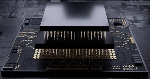
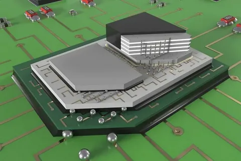
This expansion is becoming more prominent as traditional transistor scaling approaches its physical limits that forcing semiconductor companies to adopt advanced packaging technologies. It involved such as 2.5D/3D integration, chip let-based architectures and fan-out wafer-level packaging (FO-WLP). These solutions enable to provide higher interconnect density with improved bandwidth for reduced latency and better thermal performance making them essential for modern high-performance applications.
AI-Driven Computing and Chiplet Architectures Transforming Semiconductor Design
The market is witnessing for notable adoption of advanced packaging technologies due to the rapid expansion of artificial intelligence and data-intensive workloads. Even the chiplet-based architectures are emerging as a transformative approach to allowing semiconductor companies to integrate multiple functional dies into a single package for enhanced performance and flexibility.
Within the market high-performance computing and cloud infrastructure are demanding ultra-high bandwidth and low-latency communication between chips. It is become possible only through advanced packaging techniques such as 3D stacking and interposer-based integration.
Key advancements include:
• Rapid adoption of chiplet-based semiconductor architectures
• Increasing deployment of 2.5D and 3D packaging technologies
• Rising demand for high-bandwidth memory (HBM) integration
• Expansion of AI accelerators and data center processors.
These innovations beneficial for significantly improving computing efficiency while it enables for provide support to scalable and modular semiconductor design.
Rising Demand from Electric Vehicles and Automotive Electronics Accelerating Growth
In automotive industry is emerging sector led to growth driver within advanced semiconductor packaging which particularly with the rapid adoption of electric vehicles and advanced driver-assistance systems (ADAS). In modern vehicles require highly reliable also compact and thermally efficient semiconductor components to support complex electronic systems.
In the advanced packaging solutions such as system-in-package (SiP) and embedded die technologies are increasingly being used to meet these requirements. These growing integration of sensors, processors and power electronics in vehicles is further fueling demand.
Key demand drivers include:
• Expansion of EV powertrain and battery management systems
• Increasing adoption of ADAS and autonomous driving to the technologies
• Growing semiconductor content per vehicle
• Need for high-reliability and heat-resistant packaging solutions
This trend is contributing to captured positions in the advanced packaging as a critical enabler of next-generation automotive innovation.
Supply Chain Constraints and Geopolitical Pressures Influencing Market Expansion
Despite holding notable growth prospects but still the advanced semiconductor packaging market has faced several structural challenges. It involves concerns such as high capital investment requirements for advanced packaging facilities remain a major barrier with limiting participation to large, well-funded players.
In the global level supply chain remains concentrated in regions such as Asia particularly in Taiwan and China creating vulnerabilities related to geopolitical tensions. During the uncertainty in globally those create restriction on trade and export controls so these factors are contributing to cost pressures and supply chain disruptions.
Key challenges include:
- High upfront investment in advanced packaging infrastructure
- Dependence on geopolitically sensitive manufacturing hubs
- Export controls and trade policy uncertainties
- Supply chain fragmentation and rising operational costs
Within this industry address these issues due to these continuous going concern governments and companies are increasingly their investing in localized semiconductor ecosystems and diversifying supply chains.
Shift Toward Hybrid Bonding and Next-Generation Integration Technologies
The major trend contributes to shaping the market is the rapid advancement of hybrid bonding and next-generation 3D integration technologies. Hybrid bonding has enables for direct chip-to-chip connections without traditional interconnects significantly improving performance and reducing energy consumption.
In emergence of UCIe (Universal Chiplet Interconnect Express) standards is further accelerating the development of open chiplet ecosystems. It is enabling for interoperability and modular semiconductor design. Increasing innovations in glass substrates and backside power delivery are enhancing performance and efficiency.
Key innovation trends include:
- Adoption of hybrid bonding for ultra-high-density are interconnects
- Growth of UCIe-enabled chiplet ecosystems
- Advancements in glass substrate and interposer technologies
- Integration of backside power delivery for improved efficiency
These advancements are clearly redefining semiconductor packaging with how to enabling higher performance and greater design flexibility.
Competitive Landscape Focused on Technology Leadership and Capacity Expansion
The market is moderately consolidated, with leading players are continuous taking efforts for expanding advanced their own packaging capacity and making their own technological capabilities. Globally many companies are ready for strategic investments in R&D and forming partnerships to accelerate innovation in heterogeneous integration and chiplet-based solutions.
Key Players:
- ASE Technology Holding
- Amkor Technology
- JCET Group
- Intel Corporation
- Taiwan Semiconductor Manufacturing Company
These companies shifted their focus on how to build strong scaling 2.5D/3D packaging also enhancing chiplet ecosystem partnerships with local players and expanding global manufacturing footprints to maintain competitive advantage.
Transition Toward Scalable and Heterogeneous Semiconductor Ecosystems
This industry is entering a new phase which driven by the convergence of design innovation and manufacturing advancements. Within the heterogeneous integration is becoming the foundation for future semiconductor architectures enabling the combination of multiple chips into a single high-performance package.
Looking ahead towards creating emerging opportunities such as photonics-integrated packaging and modular chiplet marketplaces are expected to unlock new revenue streams. These innovations will support ultra-fast data transmission and flexible semiconductor design for catering to evolving industry requirements.
Increasing continuous advancements in packaging technologies with availability of investments and strong demand from AI, automotive, and data center applications. This advanced in semiconductor packaging market is poised to play a critical role in shaping the future of global semiconductor value chains.